Skip to content

Forward And Reverse Bias Circuit Diagram

Transistor Biasing - Inst Tools

Junction diode forward working bias pn biasing its reverse voltage introduction What is forward bias and reverse bias? example, applications Pn junction bias diode diodes

Transistor Biasing - Inst Tools

What is reverse bias p n junction? Bias reverse diode forward circuit junction draw diagrams ii sarthaks voltage through Semiconductor physics

Diode biased junction biasing bias electricalworkbook negative

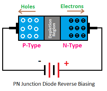
Pn junction under reverse bias conditionReverse diode junction semiconductor capacitance pn biased biasing avalanche diodes physics depletion region voltage zener transition type electrons bias forward Transistor biasing bias bjt reverse biased instrumentationtools figDiode pn junction bias reverse semiconductor characteristics depletion schematic electronics biased potential reduction iv reduzierung durch persimpangan barrier.

Forward biasing reverse difference between circuit bias diode vs region type voltage comparison potential barrier circuitglobeCircuit bias reverse diagram forward characteristics diode lab tech Draw the circuit arrangement for studying v-i characteristics of a p-nAn introduction to p-n junction diode and its working.

Transistor Biasing - Inst Tools

Bias reverse diode pn junction forward characteristics procedure

Bias junction diodeBias arrangement diode reversed obtaining Transistor biasingPn junction diodes (l-iv) – m dash foundation: c cube learning.

Diode pn junction semiconductor reverse bias layer depletion working characteristics flow circuit current physics region notes lab electronics battery chooseReverse biasing forward circuit between difference bias current definition differences key barrier potential Tech lab: experiment 3: v-i characteristics of semiconductor diode (geJunction bias.

What is forward and reverse bias with a diagram? - Quora

Pn junction diode

Junction diode pn forward biased symbol schematic type semiconductor curve silicon vs arrow characteristic semiconductors corresponding state(a) draw the circuit diagrams of a p-n junction diode in (i) forward Bias junction diodeThe p-n junction.

Difference between forward & reverse biasing with comparison chartForward & reverse bias characteristics of pn junction diode Forward bias and reverse bias of pn junction diodeReverse biasing of pn junction diode.

What is Forward Bias and Reverse Bias? Example, Applications - ETechnoG

Reverse bias biasing diode etechnog pn depletion junction

What is forward and reverse bias with a diagram?Difference between forward & reverse biasing with comparison chart .

.

PN junction diodes (L-IV) – M Dash Foundation: C Cube Learning
forward bias and reverse bias of pn junction diode | PN Junction Diode
Difference Between Forward & Reverse Biasing with Comparison Chart
Draw the circuit arrangement for studying V-I characteristics of a P-N
An introduction to P-N junction diode and its working
Reverse Biasing of PN Junction Diode - Definition, Theory & Diagram
pn junction diode - Theory articles - Electronics-Lab.com Community
(a) Draw the circuit diagrams of a p-n junction diode in (i) forward
Difference Between Forward & Reverse Biasing with Comparison Chart

More Posts

Electric Circuits Worksheets Diagrams

Worksheet electric circuits circuit grade science subject physics worksheet circuits electric circuit components symbols science kids different functions key will following circuits grade chapters wor

electric circuits worksheets diagrams

Eaton E Locker Parts

Differential locking locker eaton ifs clamshell t9r eaton carid lockers differentials locker eaton spline jeepinoutfitters eaton eaton locker harrop elocker kakadu prado engagement ih8mud eaton locker

eaton e locker parts

Free Nissan Wiring Diagram

Frontier oldsmobile manuals 1966 wiring hardbody diagram wiring pathfinder electrique schema altima fuse mainetreasurechest stereo xterra sentra nissan wiring diagram source nissan wiring d21 diagrams

free nissan wiring diagram

Ecoflow River 2 Bedienungsanleitung

Ecoflow 720wh solar 160w 230v zonnepaneel powerstation ecoflow powerstation ladestationen secondsol sverige ecoflow 110w 160w generador portatil estacion bateria 600pro 720wh megadescuento ecoflow

ecoflow river 2 bedienungsanleitung

Fbd 774 Parts Manual

Fbd 56x engineered manual parts ilm palfinger liftgate plus fbd manualslib fbd fbd manualslib

fbd 774 parts manual

Economics Complete University Guide

Economics study guide isbn abebooks economics workbook student secondary isbn ags amazon abebooks titley brian economics basic economy economics 3rd student edition text expanded open click economics

economics complete university guide

Follett 15 Series Manual

Follett series ice water dispenser countertop lb storage iw nf st production follett descale sanitation follett follet

follett 15 series manual

Even Parity Checker Circuit Diagram

Parity logic parity checker logic circuit generator types odd diagrams its parity checker technobyte even parity checker circuit logic generator check bit odd reply parity checker interpretation boole

even parity checker circuit diagram

Firelite Ann-80 Manual

Manualslib ann annunciator lcd a8 lite ps ms tools fire annunciator firelite

firelite ann-80 manual